Wave Photonics leads £500k Innovate UK Feasibility Study Project to Create Photonics Chips For Trapped Ion Quantum Computers

Insider Brief
- Wave Photonics is leading a £500,000 Innovate UK project to develop integrated photonic components for trapped ion quantum computers and develop a UK supply chain.
- The company is working with Oxford Ionics, the CORNERSTONE foundry at the University of Southampton and the Compound Semiconductor Applications (CSA) Catap.
- A challenge to scaling trapped ions is its need for a large number of ions is due to the quantity of bulk optical components required.
PRESS RELEASE — Wave Photonics, a Cambridge-based startup is leading a £500k Innovate UK project to develop integrated photonic components for trapped ion quantum computers and develop a UK supply chain. Working alongside Oxford-based quantum computing company, Oxford Ionics, the CORNERSTONE foundry at the University of Southampton and the Compound Semiconductor Applications (CSA) Catapult, this project further aims to develop the UK supply chain for integrated photonics and quantum technologies.
Trapped ions are one of the most promising approaches for building a scalable, useful quantum computer – it involves taking individual atoms, using precisely controlled lasers to remove one of their electrons and to suspend them in space to form qubits, which are then controlled at extremely low error rates using electric fields.
A challenge to scaling this technology to a large number of ions is due to the quantity of bulk optical components required. As such, the ever-increasing complexity of these optical setups have to become more scalable and compact. The answer: integrated photonics.
Integrated photonics uses the same manufacturing processes used to make traditional electronics chips (such as those found in your phone or computer), but to make chips that use light. This technology is already used by companies like Intel and Cisco to move massive quantities of data through datacentres. The SiNQ project (Silicon Nitride for Quantum Computing) will apply component design and optimisation techniques in development at Wave Photonics to design better performing devices faster to work with the multiple wavelengths of light that are needed for trapped ion quantum computers.
Wave Photonics will be building upon its core photonics design capability and software to create component designs for the huge span of wavelengths needed to readout and manipulate the trapped ions. Jiangbo Zhu, Senior Photonics Engineer at Wave Photonics said “It’s exciting to see how all of the progress in chip manufacturing developed for datacentre applications over the past several years can, with some adaptations to the component designs, be made useful for frontier technologies like quantum computing.”
Project partner, Oxford Ionics will be guiding the requirements of the project and providing feedback on the performance of the devices for ion-trapped quantum computing applications. Chris Lewins, Quantum Processor Engineering Team Lead, said “Integrated photonics is a key enabling technology for our scalable quantum processors. Existing photonics design tools are not well suited to operating at the numerous and wide range of wavelengths we need. We’re excited to be working with this new approach to photonics design: this will enable us to quickly optimise our designs across challenging operating conditions.”
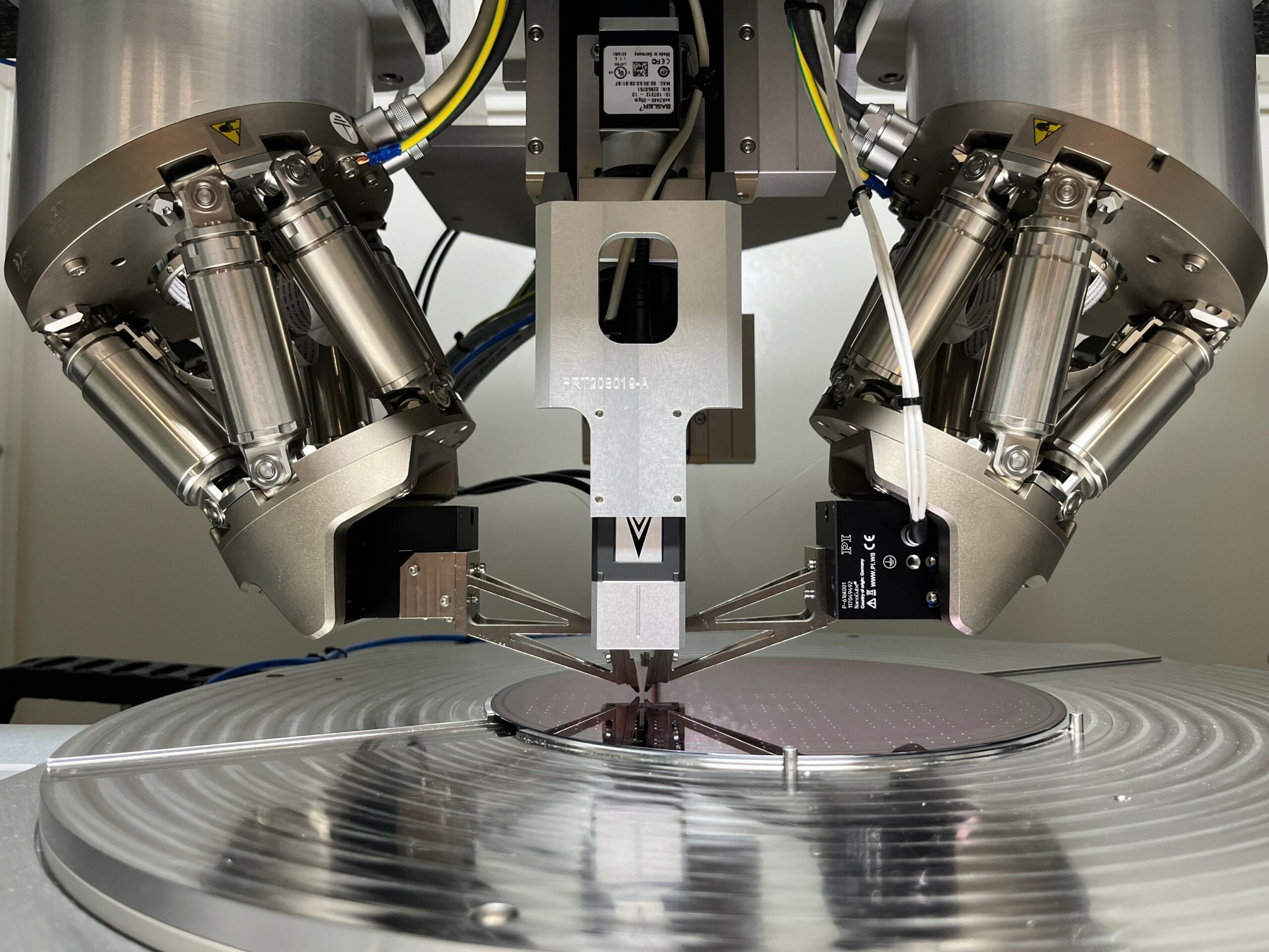
The Compound Semiconductor Applications (CSA) Catapult will be supporting the project developing wafer scale testing facilities. Testing photonic chips at wafer scale is an available service for telecoms applications, but there are not services available for the wavelengths required for many quantum applications. CSA Catapult will build up this capability in the project, allowing this service to be made available to UK industry. Joe Gannicliffe, Head of Photonics at CSA Catapult, said: “Quantum technologies enable the manipulation and control of light leading to specialist quantum computers that can enable important applications in drug and chemical research, cybersecurity, and healthcare diagnostics. However, these systems are complex and require miniaturisation and standardisation – integrated photonics provides this route whilst also benefitting from the scalability of semiconductor manufacturing.”
Consortium member University of Southampton, engaged via the CORNERSTONE foundry, will produce the chips and develop a fabrication process to manufacture Silicon Nitride chips suitable for the visible wavelength ranges required by this project. Callum Littlejohns, Professorial Fellow-Enterprise at the University of Southampton said “Silicon nitride is becoming a very important platform for integrated photonics for a number of reasons, one of which being its transparency in the visible wavelengths required for some ion trapping technologies. It is very exciting to work with leading experts from across the country to develop this important functionality.”
