
New X-ray Technique Helps Scientists Watch Quantum Materials Respond to Laser Pulses
Insider Brief
- Argonne researchers developed an X-ray imaging technique to track silicon carbide’s response to ultrafast laser pulses, providing insights that could improve the precision of creating quantum defects.
- The measurements revealed energy moving through the crystal as fast mechanical waves and more slowly dispersing heat, capturing changes across its surface and into its interior.
- The technique could help researchers refine laser conditions to create more reliable defects for use as qubits, though precise placement remains a long-term goal.
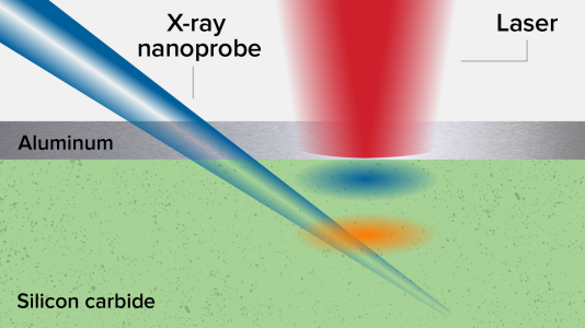
- Image: In a new technique developed at Argonne, an X-ray beam is directed at silicon carbide at a controlled time after the material is struck by a pulse of laser light. The X-ray acts like a camera, letting scientists see in real time how the material responds to the laser. (Haidan Wen/Argonne National Laboratory)
PRESS RELEASE — Creating a quantum device often begins by intentionally damaging a crystal.
Scientists fire an ultrafast laser pulse into a material, knocking atoms out of place and leaving behind tiny imperfections called vacancies. Far from being flaws, these vacancies can behave as qubits — the fundamental building blocks of quantum information.
The challenge is precision.
Researchers want to place these quantum defects exactly where they need them, but until now they have had only a limited understanding of what happens inside a crystal during the instant when a laser creates the defect.
Scientists at the U.S. Department of Energy’s (DOE) Argonne National Laboratory have now taken an important step toward solving that problem.
Using the Advanced Photon Source (APS), a DOE Office of Science user facility, the team developed a new X-ray imaging technique that lets them watch, in three dimensions and in real time, how silicon carbide responds immediately after an ultrafast laser pulse strikes it. Their work provides real-time pictures of how the laser’s energy moves through the material — a key step toward building quantum devices with atomic precision.
The research appears in ACS Nano and was supported by Q-NEXT, a DOE National Quantum Information Science Research Center led by Argonne.
“Before you can precisely engineer quantum defects, you have to understand exactly what the laser is doing inside the material,” said Argonne scientist Haidan Wen, an author of the paper. “This technique lets us watch that process unfold, especially how atoms move in ways that weren’t possible before.”
Building better quantum materials
Drawing on the special features of quantum physics, quantum information technologies are expected to give us new ways to share information. They could speed drug discovery, help protect financial transactions and deliver solutions to currently intractable problems using quantum computation. The foundation of these technologies is the qubit.
Silicon carbide has emerged as one of the most promising qubit materials. It’s capable of hosting atomic-scale defects whose quantum states can store and process information. And it is already widely used by the semiconductor industry, making it an attractive platform for manufacturing future quantum technologies at scale.
Scientists create the defects by striking the crystal with ultrafast laser pulses lasting only millionths of a billionth of a second.
Compared with earlier methods that relied on electron or ion beams, lasers offer the possibility of creating vacancies at carefully chosen locations inside the crystal. But researchers have not fully understood exactly how the energy travels through the material before a vacancy forms.
“Our long-term goal is deterministic defect creation,” Wen said. “We want to be able to place a quantum defect exactly where we intend it to go every time.”
Using X-rays as a camera
To better understand the process, the researchers turned to the APS, one of the world’s brightest X-ray sources.
Their approach combines an ultrafast laser with an exceptionally small, highly focused X-ray beam. The laser initiates the process, while precisely synchronized X-ray pulses act like a camera, recording how the crystal responds over time.
Unlike visible light, hard X-rays penetrate deep into the material while remaining sensitive to the positions of individual atoms. That allowed the researchers to observe structural changes occurring beneath the surface — something conventional optical techniques cannot easily accomplish. Researchers used Argonne’s Center for Nanoscale Materials — another DOE Office of Science user facility — to interpret the X-ray diffraction patterns, using them to measure how the silicon carbide changed.
The team also achieved exceptionally fine spatial resolution by focusing the X-ray beam to hundreds of nanometers across — a hundred times thinner than the width of a human hair.
“This gives us a way to see not only what’s happening on the surface, but also how the response evolves deep inside the crystal,” said Argonne scientist Stephan Hruszkewycz, one of the paper’s authors. “That depth information has been missing, and it’s essential for understanding how laser-written quantum defects form.”
Following energy through the crystal
The measurements revealed two distinct ways that energy travels after the laser pulse.
Part of the energy moves rapidly through the crystal as an organized mechanical wave, similar to ripples spreading across a stretched surface after it is struck. At the same time, some of the energy slowly disperses as heat, causing nearby atoms to vibrate randomly before the crystal gradually returns to equilibrium.
For the first time, the researchers were able to directly image how these different energy-transport processes evolve both across the surface and into the depth of the material. Being able to image energy’s propagation from the crystal’s surface to the interior introduces a level of detail previously out of reach.
To visualize the process, imagine dropping a bowling ball onto a hefty rubber slab. The impact sends a ripple through the material. The laser creates a similar disturbance inside the crystal, and the APS serves as an ultrafast camera, capturing a sequence of X-ray images that reveal how the disturbance spreads and fades billionths of a second after the laser strikes.
Understanding this behavior could eventually help scientists fine-tune laser-writing conditions to produce more reliable quantum defects.
“Every improvement in our understanding brings us closer to engineering quantum materials instead of discovering them by trial and error,” Hruszkewycz said.
A platform for future discoveries
Although the study focused on silicon carbide, the researchers say the imaging approach can be adapted to many other materials used in quantum information science.
The work also highlights the unique capabilities available at the APS, where advanced X-ray optics, ultrafast laser systems and precise timing electronics make experiments like this possible.
For Argonne, which combines expertise in quantum information science with world-class materials characterization, the project demonstrates how new measurement tools can accelerate the development of future quantum technologies.
The ability to watch materials respond in real time does not itself create better qubits. But by revealing the physical processes that govern their formation, it gives scientists the knowledge needed to improve how they manufacture them.
“Our goal isn’t just to observe these processes,” Wen said. “It’s to learn enough from them that we can eventually build quantum devices with the level of precision that practical quantum technologies will require.”
Co-authors with Hruszkewycz and Wen are Kumar Neeraj, Matthew J. Highland, Tao Zhou, Burak Guzelturk, Donald A. Walko, Nathan C. Flanders, Nazar Delegan, F. Joseph Heremans and Martin V. Holt.
This material is based upon work supported by the DOE’s Office of Science National Quantum Information Science Research Centers as part of the Q-NEXT center.